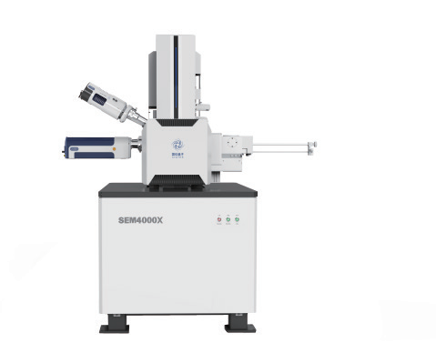
Field Emission Scanning Electron Microscope
Field emission scanning electron microscopes (FE-SEM) are essential in materials science, semiconductor inspection, and life sciences for their high-resolution imaging. Leading manufacturers partner with top global research institutes and tech firms, driving advancements in low-voltage imaging and automated analysis. With strong production capabilities and rigorous quality control, industry leaders ensure reliable supply. Global FE-SEM sales are growing steadily, fueled by demand in nanotechnology and advanced research. Due to high customization, production is largely order-based, with limited whole-unit inventory, though key components are kept in stock to maintain production flexibility and support ongoing innovation.
- HC
- CHINA
- 1 CHINA
- 200/ MONTH
- Information
- Download
Core Applications and Industry Status of Field Emission Scanning Electron Microscopes in Modern High-End Detection Fields
The Field Emission Scanning Electron Microscope (FE-SEM) serves as a critical tool for nanoscale characterization, with its core technological advantage lying in the use of a field emission electron source to acquire ultra-high-resolution microscopic images. Compared to traditional thermionic emission electron microscopes, the Field Emission Scanning Electron Microscope features an electron beam with higher brightness and lower energy spread. This enables the Field Emission Scanning Electron Microscope to achieve clearer and more authentic surface topography observations on non-conductive or beam-sensitive samples. Currently, the applications of the Field Emission Scanning Electron Microscope have deeply penetrated numerous cutting-edge fields such as semiconductor manufacturing, new material research and development, life sciences, and geology/archaeology. In the semiconductor industry, the Field Emission Scanning Electron Microscope is crucial for defect inspection and dimensional metrology of chip structures. In materials science, the Field Emission Scanning Electron Microscope helps researchers analyze the relationship between a material's microstructure and its properties. In the field of biology, appropriately prepared biological samples can also obtain detailed three-dimensional surface information through the Field Emission Scanning Electron Microscope operating in low-voltage mode.
The technological development of the Field Emission Scanning Electron Microscope has always centered on enhancing performance and expanding functionality. Modern Field Emission Scanning Electron Microscopes not only pursue extremely high spatial resolution but are also dedicated to integrating various analytical detectors, such as Energy Dispersive X-ray Spectrometers (EDS) and Electron Backscatter Diffraction (EBSD) systems, enabling simultaneous acquisition of micro-area compositional and crystallographic information. The sample chamber design of the Field Emission Scanning Electron Microscope is also becoming increasingly flexible, capable of accommodating larger samples or integrating attachments for in-situ stretching, heating, and other stimuli. This allows the Field Emission Scanning Electron Microscope to dynamically observe the evolution of a material's microstructure under external excitation. These technological advancements have transformed the Field Emission Scanning Electron Microscope from a pure imaging device into a comprehensive micro-analysis platform. Automation and intelligence are also significant trends for the Field Emission Scanning Electron Microscope. Through advanced image recognition and automated navigation software, the Field Emission Scanning Electron Microscope can greatly improve inspection throughput and data analysis efficiency.

From an industry chain perspective, the research, development, and manufacturing of the Field Emission Scanning Electron Microscope are concentrated among a few internationally renowned scientific instrument companies that possess core technologies. These companies drive the continuous breakthrough of various parameters of the Field Emission Scanning Electron Microscope through sustained R&D investment. The production of the Field Emission Scanning Electron Microscope involves the integration of precision electron optical systems, ultra-high vacuum systems, high-sensitivity signal detection systems, and complex control software. The manufacturing process is intricate, and the technological barriers are extremely high. Consequently, the global market for the Field Emission Scanning Electron Microscope exhibits a highly concentrated structure. Downstream users are primarily top universities, national-level research institutions, and the R&D and quality control departments of high-tech industries (such as integrated circuits and new energy batteries). Procurement decisions for the Field Emission Scanning Electron Microscope are typically based on its resolution, stability, analytical expansion capabilities, and the long-established technical reputation of the brand.

Regarding the market performance of the Field Emission Scanning Electron Microscope, demand for the Field Emission Scanning Electron Microscope maintains steady growth alongside increasing global investment in nanotechnology and precision manufacturing. Particularly in areas like advanced process chip R&D and secondary battery material development, higher demands are placed on the performance of the Field Emission Scanning Electron Microscope, which also drives sales of high-end Field Emission Scanning Electron Microscopes. As the Field Emission Scanning Electron Microscope is a high-value, high-technology-density capital equipment, its sales model is primarily based on direct orders with strong production planning. Manufacturers typically maintain a certain inventory of key components to ensure supply chain resilience. However, the inventory of complete Field Emission Scanning Electron Microscope units is generally low, with most being assembled and tested according to specific configuration requirements from customers. This model ensures that the Field Emission Scanning Electron Microscope can be flexibly adapted to users' personalized needs while also requiring manufacturers to possess efficient supply chain management and precise production scheduling capabilities.


